State of the Art Controllers for industrial applications
21 September 2018Latest modification: 3 February 2022
Introduction
GOODRAM Industrial mass storage devices for industrial applications are characterized by high reliability, durability and a wide operating temperature range. These features are achieved by designing based on customer’s specifications and expectations. It would be impossible without the proper selection and validation of the components. During this process, a special attention is paid to the memory controller and its features, which results in a failure-free operation over a long period of time.
FLASH Management
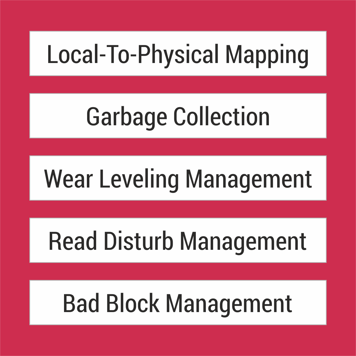
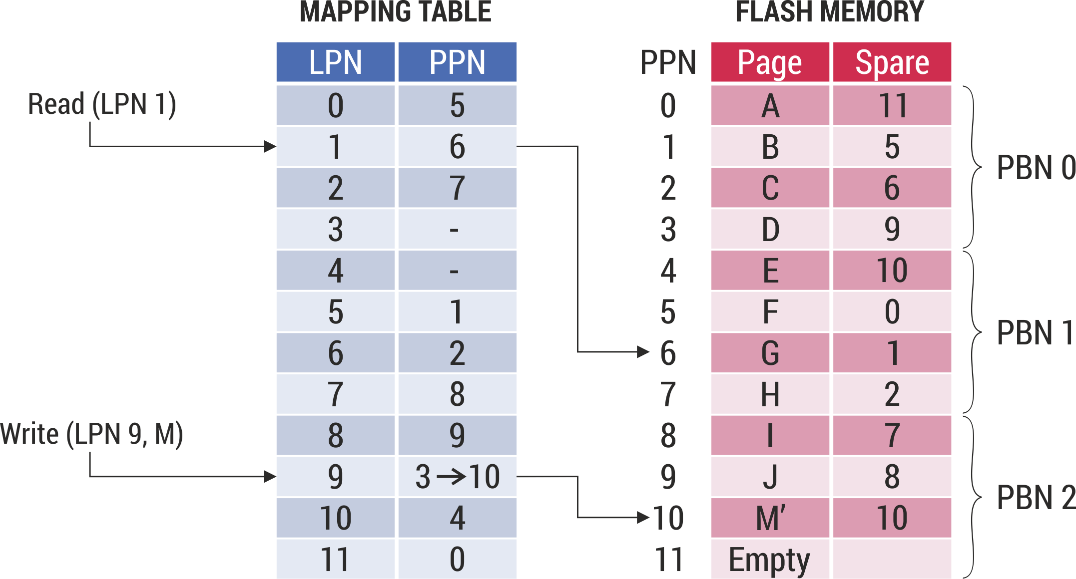
The use of NAND flash in mass storage requires a number of optimization techniques.  One of the most important techniques of optimization is a translation of drive’s sector address to physical address of memory page (logical to physical mapping). It is crucial, because the host (computer), addresses the memory using 512B sectors, while the size of a typical NAND flash page is 8 or 16 kB and it is not possible to program the page again without deleting the entire memory block. The memory block contains between 256 and 512 pages, so the address translation mechanism, must cooperate with the garbage collection algorithm. Garbage collection involves defragmentation of memory blocks. As a result, the current data is transferred to free memory pages to fill the block. The block that contains obsolete data is deleted and prepared for rewriting. An even distribution of write cycles between all NAND flash memory blocks is provided by the wear leveling algorithm. It is based on the program/erase (p/e) cycle counters of the memory blocks. All of the mentioned algorithms, take into account the map of damaged blocks. This map is created at the moment of mass storage initialization and can be extended at a later time by blocks excluded from use, called run time bad block or later bad block. The build quality and high reliability of the optimization algorithms implemented in GOODRAM Industrial products, guarantee a trouble-free storage operation over the entire specified period of use.
Flash translation layer
SSD controllers use page mode mapping flash translation layer. During the write and read of data sector, the logical page number (LPN) is calculated. The logical page number is translated into the physical page number (PPN). The translation is performed using the mapping table.  The mapping table stores information that allows to select the right memory chip, core, physical memory block (PBN – physical block number). The advantage of page mapping mode FTL is high speed and low write amplification. WIn SD card controllers, there’s a second method of translation called block mode mapping. The principle of block mapping mode is similar to the method discussed earlier, only the mapping table includes block addresses. The choice of translation method depends on the NAND flash memory chip used and the expected operation speed.
Wear leveling
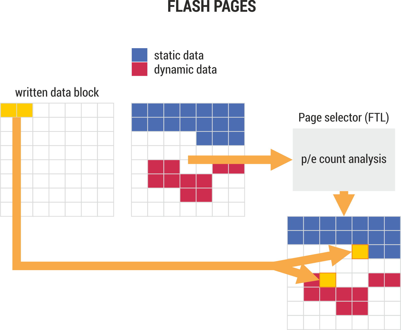
 All GOODRAM Industrial storage controllers incorporate a static and dynamic wear leveling algorithms. The core strategy of the wear leveling algorithm is to select memory blocks in such a way as to reduce the differences between the number of p/e cycles in all memory blocks. This target is achieved by changing the location of static data and using these locations to store frequently moving data.
Over Provisioning
Over provisioning is supported by all controllers used in GOODRAM Industrial mass storage products. In case of SSD and operating systems supporting the TRIM command, the size of dynamic overprovisioning depends on the layout of partitions on the drive i.e. the space not allocated to the partition or the space to which files are not allocate is automatically used by the controller to increase the performance and durability of NAND flash. The area dedicated for overprovisioning can also be set by the user, using any disk tool and ATA SET MAX ADDRESS command, e.g. hdparm (Linux). In case of the SD card controller it is not possible to set overprovisioning. In this case, increasing card performance and durability can be done by deleting data sectors before overwriting them again (ERASE – CMD38 command).
ECC
SSD and SD card controllers use BCH and LDPC hard and soft decoding and error correction methods. The BCH method (S10, SD controllers) is used for 2D planar memory. The LDPC method is used to detect and correct errors in 3D NAND (in case of S11, also 2D NAND). In the case of SSD controllers, additional ECC bits are generated, which are stored in memory pages other than data pages (ECC RAID). If an uncorrectable error is detected, additional ECC bits, increase the probability of correcting errors. If this happens, the corrected data is stored in another page, and the block that contains the original page is marked as bad.
Read-retry
 If uncorrectable errors occur, controllers implemented within the GOODRAM Industrial mass storage products will try again to read the data for the changed reference voltage value Vref. The read data is subject to hard correction (BCH, LDPC hard algorithm) or can be used to create voltage distribution statistics. Voltage distribution statistics are the basis of the LDPC soft decoding algorithm.
Sudden Power loss protection
The risk of data loss due to a sudden power failure is minimized by methods appropriate for a given controller. In S10 and S11 controllers, a strategy is implemented to limit the amount and duration of data retention in the cache memory. The ACK signal that confirms data is saved is only generated after data has been written to the main flash memory. This eliminates the risk of false positive confirmation of data write. Furthermore, in the case of the S10 controller, it is possible to maintain the power supply through tantalum capacitors. This function is optional and requires the design of additional electrical circuits. SD card controllers follow a different strategy by executing double write cache. When the power supply is switched on, the last recorded data is verified. If uncorrectable data errors occur as a result of a power loss, overwriting of the original data is omitted or the data is retrieved from the buffer.
SmartZIP
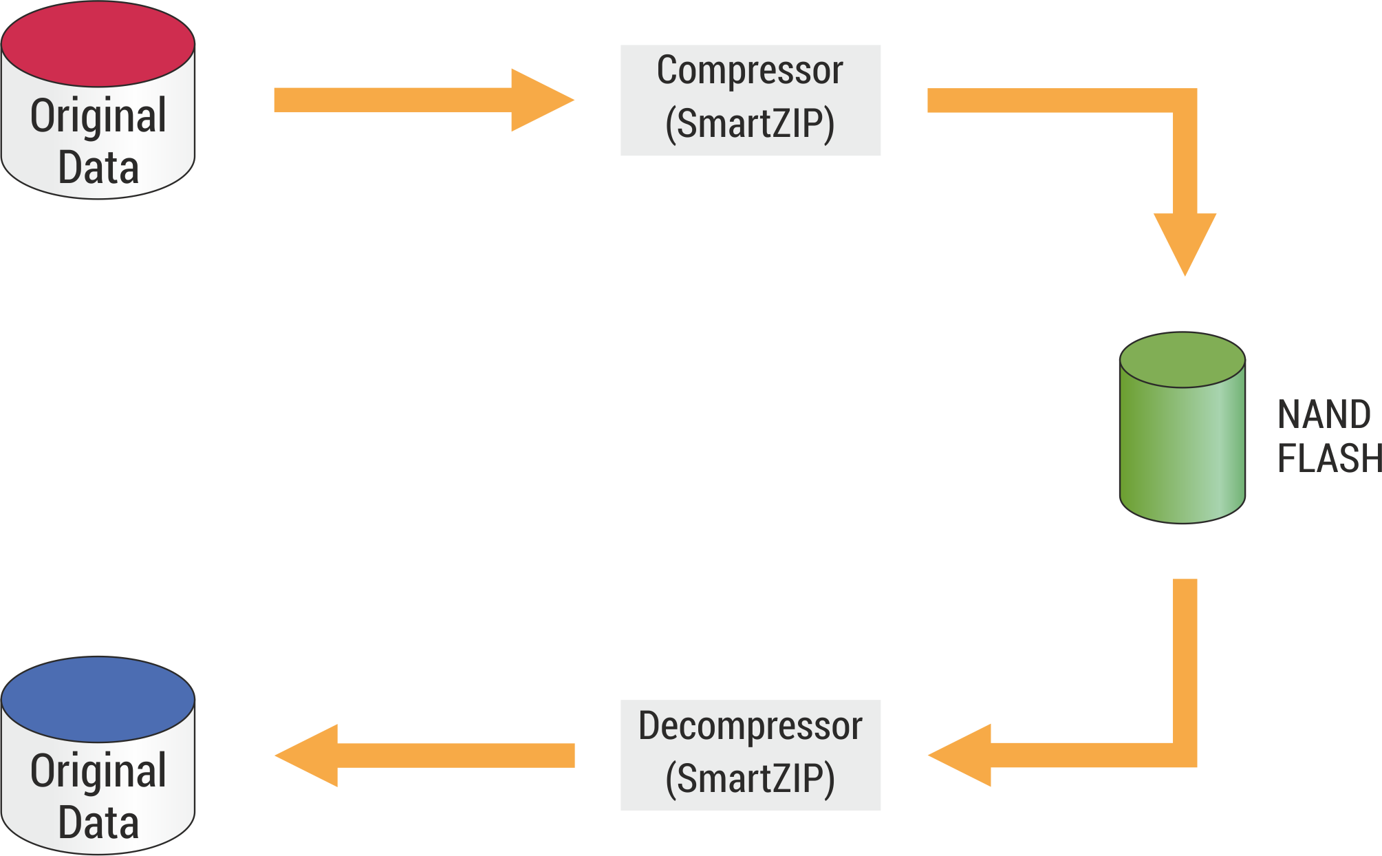
SmartZIP works by compressing data in the write cycle and decompressing data in the read cycle. In the write cycle, data from the write buffer is directed to the compression block. In the compression block its size is reduced. Depending on the entropy, the size of saved blocks can be reduced several times. The compressed data is stored in NAND flash. During the read cycle, the opposite situation occurs, i.e. the data read from NAND flash is decompressed and then transferred to the read buffer. The advantages of SmartZIP function are high speed (compression is performed internally without host intervention) and extension of NAND flash endurance.

Controllers comparison
| Phison PS3110-S10 | Phison PS3111-S11 | Phison PS8210 | |
|---|---|---|---|
| Interface | SATA III | SATA III | SD 3.0 |
| FLASH type | MLC, TLC, 3D NAND | 3D NAND, TLC, MLC | 3D NAND, TLC, MLC |
| FLASH channels | 8 | 2 | N/A |
| ECC type | BCH | LDPC hard&soft decoding | BCH, LDPC hard&soft decoding |
| RAID ECC | YES | YES | NO |
| FTL | page mapping mode | page mapping mode | block/page mapping mode (depend on FLASH&application) |
| DRAM cache | up to 1GB | DRAM less | N/A |
| Encryption | supported | supported | supported |
| Data compression | NO | YES | NO |
| Capacity | up to 1TB | up to 512GB | up to 512GB |
| R/W speed (seq) | 550/520 MB/s | 550/500 MB/s | 90/45 MB/s |
| R/W speed (rand 4kB) | 100k/90k IOPS | 100k/85k IOPS | N/A |
| Sudden power loss management | YES, high capacitator optionally available | YES | Software based |
| SMART attributes | YES | YES | YES (optional) |
| NCQ | 32 deep | 32 deep | N/A |
| TRIM | ES, depends on FW deterministic/non-deterministic | YES, depends on FW deterministic/non-deterministic | N/A |
| Secure Erase | YES | YES | N/A |
| Over provisioning | YES | YES | YES |
| Thermal sensor and thermal event | supported (optionally) | supported (optionally) | N/A |
| Bad block management | build in + later | build in + later | build in + later |
| Low power management | DIPM/HIPM Mode | DIPM/HIPM Mode | according to SD standard |
| Read retry | YES | YES | YES |